APi was founded on extensive research in semiconductors, optical communications, and optical interconnects led by Professor Yoshiaki Nakano at the University of Tokyo’s Research Center for Advanced Science and Technology (RCAST).
APi focuses on the global market and develops highly competitive products that aim to set new international standards.
APi continuously explores the limitless potential of photonics, creating new value and contributing to the advancement of society and humankind.
APi is managed under a philosophy that harmonizes employee motivation with the company’s growth and profitability, while ensuring fair returns to its shareholders.
2023/10
Obtained TUV & cTUVus Certifications for all the isolator chip products. Link . Link
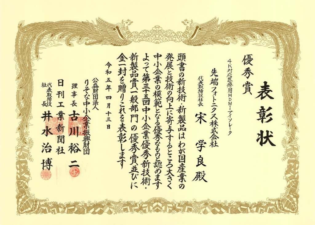
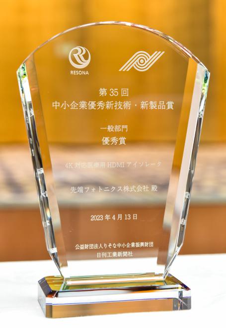
2023/4/13
Our HDMI 2.0 Isolator received the Excellence Prize (General Category) at the 35th Excellent New Technology and Product Awards for Small and Medium Enterprises, organized by the Resona Foundation and The Nikkan Kogyo Shimbun.
Link1Link2
2022/2/8
Obtained IEC 60601-1 compliance test reports from Intertek for USB 3.0 and HDMI 2.0 Isolator chips. Link . Link
2021/7/1
Release of the HDMI 2.0 Isolator chip. Link
2020/9/3
We've posted an editorial advertisement for our USB 3.0 isolator chip in the EETimes.
Link
2020/5/1
Release of the USB 3.0 Isolator chip. Link
2017/5/22
Sony’s F65 CineAlta Camera, which APi collaborated in the optical data transmission technology, was honored Academy’s Scientific and Engineering Awards. Link-1Link-2
2016/2/8
In the technical private show held by KT Group during 19th to 20th April, APi demonstrated a tiny high-resolution POF camera co-developed with KT Group and Honda Tsushin Kogyo Co., Ltd. Link-1Link-2(5/22 added)
POF: Plastic Optical Fiber
2016/2/8
APi has released 100 Gbps Infiniband EDR QFSP+ AOC.
For more information, click here. (PDF file)
2014/11/19 - 11/21
Exhibitor at the "New Value Creation Exhibition 2014". APi will be exhibiting our products and technologies at the "New Value Creation Exhibition 2014" in Tokyo, in the Big Site convention facilities. This is to be held in November, for three days (19th to the 21st).Please come visit our booth situated near the entrance 'East Hall 2, 3' http://shinkachi.smrj.go.jp/
2014/4/24
On April 24th, 2014, APi was given coverage in the Nikkei Business Daily (The Nikkei Sangyo Shimbun, a cutting-edge industry newspaper issued by Japan most influencial publishing group).
For details, please refer to here (pdf file)
2013/9/12
On Sept. 12th, 2013, APi was given first-page top coverage in Nikkan Kogyo Shimbun (a well established leading business & technology daily newspaper in Japanese language) for article titiled "100 Gigabit per second Optical Fiber Cable for Communication shows bright prospects for practical implementation".
For details, please refer to here (pdf file)
2013/3/30
On Mar. 30th, 2013, APi was covered in the evening edition of Nihon Keizai Shimbun (a leading daily newspaper on economic and financial matters with large worldwide circulation, issued by Japan most influencial publishing group).
For details, please refer to here (pdf file)
2012/6/13-15 Exhibitor at the 'Large Electronics Show 2012' APi will be exhibiting our new products and technologies at the “Large Electronics Show 2012” in Tokyo, in the Big Site convention facilities. This is to be held in June, over three days (13th to the 15th). Please come and visit us at our booth (50-1), situated near the entrance ‘East Hall 6’.
2012/6/6-7 Please come and visit our exhibition at the "ADVANTEST EXPO 2012". This will be held in the Tokyo International Forum, on the 6th and 7th of June 2012. We will be exhibiting our new products and technologies at our booth, in the 'Near Future/Future Zone'.
2012/5/1
Sony has recently announced a professional use movie camera, 'CineAlta F65', having the industries highest image resolution of 4K2K. This camera employs optical interconnect technology jointly developed with APi.
(Details are attached to the top column of the Media coverage) http://www.sony.co.jp/SonyInfo/News/Press/201202/12-029/
2012/4/11-13 APi will be taking part in "Photonix 2012", which is to be held from the 11th to 13th of April 2012, at the Big Site Tokyo. We will be exhibiting our products and showcasing our new technologies at our booth (28-10) situated in the right side of East Hall 4. Please feel free to come and visit us. http://www.photonix-expo.jp/en/Home/
2012/2/23
We gave an invited presentation on the MOT (Management of Technology) Special Educational Program, which was held at the Graduate School of Science and Technology in Kumamoto University, on the 23th of February. The talk was part of the venture study group business and was entitled, "How to target new markets created by technology − the challenges facing university based venture business companies". http://www.gsst.kumamoto-u.ac.jp/detail.php?type=news&tday=20120213&ttime=090729
2023/5/31 The award winners' roundtable discussion from the 35th Excellent New Technology and Product Awards for Small and Medium Enterprises was featured in The Nikkan Kogyo Shimbun. LinkLink
2023/5/31 We were featured in The Nikkan Kogyo Shimbun's "Behind the Scenes of Development" special series as a recipient of the Excellent New Technology and Product Awards for Small and Medium Enterprises. Link
2012/5/1 The world’s first mass production of a lensless optical interconnection module has been successfully achieved thanks to newly developed semiconductor technology. For details, please refer to here(PDF file)
2012/3/29
APi was showcased on the website of Tokyo Bureau of Industrial and Labor Affairs under the heading of "Bright technology: Optical Business." kirari-tech.metro.tokyo.jp
2009/10
In the October 2009 Japanese journal Electronic Packaging Technology release we released an article entitled "The development of light interconnect PCB substrate technology to facilitate a light testing system" The translation of this publication is given here (pdf file)
 Exhibitor at the 'Large Electronics Show 2012'
 This will be held in the Tokyo International Forum, on the 6th and 7th of June 2012. We will be exhibiting our new products and technologies at our booth, in the 'Near Future/Future Zone'.
 APi will be taking part in "Photonix 2012", which is to be held from the 11th to 13th of April 2012, at the Big Site Tokyo. We will be exhibiting our products and showcasing our new technologies at our booth (28-10) situated in the right side of East Hall 4. Please feel free to come and visit us.
 The award winners' roundtable discussion from the 35th Excellent New Technology and Product Awards for Small and Medium Enterprises was featured in The Nikkan Kogyo Shimbun.
  We were featured in The Nikkan Kogyo Shimbun's "Behind the Scenes of Development" special series as a recipient of the Excellent New Technology and Product Awards for Small and Medium Enterprises.
 2012/3/29
 2009/10