Top Page > Media Coverage
2023/5/31
 The award winners' roundtable discussion from the 35th Excellent New Technology and Product Awards for Small and Medium Enterprises was featured in The Nikkan Kogyo Shimbun. The article highlights the key features of the award-winning product as well as the future business plans.
Link Link
2023/5/31
 We were featured in The Nikkan Kogyo Shimbun's "Behind the Scenes of Development" special series as a recipient of the Excellent New Technology and Product Awards for Small and Medium Enterprises.
Link

2012/5/1
The world's first mass production of a lensless optical interconnection module has been successfully undertaken, due to newly developed semiconductor technology.
For details, please refer to here(pdf file)
2012/3/29
APi was showcased on the website of Tokyo Bureau of Industrial and Labor Affairs under the heading of "Bright technology: Optical Business."
kirari-tech.metro.tokyo.jp
2009/10
In the October 2009 Japanese journal Electronic Packaging Technology release we released an article entitled “The development of light interconnect PCB substrate technology to facilitate a light testing system”
The translation of this publication is given here (pdf file)
2009/05/15
Our company was covered by May 2009 issue “OPTCOM”, a magazine specialized in optical communications business.
For details, please refer to here(pdf file).
2009/05/12
Our company was taken up by May 2009 issue of “Laser Focus World Japan”, a magazine specialized in optical communications in its Features column.
For details, please refer to here(pdf file).
2008/09/16
Our company was covered by the website “Tech-On” on its Sept 16, 2008 issue published by Nikkei BP in its electronic parts technology section.
Link URL http://techon.nikkeibp.co.jp/english/NEWS_EN/20080912/157897/
2008/09/11
Advantest Corporation introduced our company as a partner for the joint development effort in its news release titled “Advantest Corp has successfully developed a new Optical PCB Technology, capable of 160 Gbps transmission” , made on 11 September 2008 in its website.
Link URL http://www.advantest.co.jp/news/press-2008/20080911/index.shtml
Advantest Corp. has successfully developed a new Optical PCB Technology, capable of 160 Gbps transmission.
~Toward commercialization of the testing system of 40 Gbps per channel, the fastest ever in the industry~Advantest Corp (head office in Chiyoda-ku, Tokyo; President: Mr.Toshio Maruyama) has recently succeeded in developing a new Optical PCB Technology to enable 160 Gbps transmission by adoption of Optical Waveguide Technology which allows 40 Gbps communications per channel. This is six times faster than the existing products of the company.Its commercialization is targeted in three years.
2008/09
SMBC Consulting Co., Ltd., a management consulting arm of Sumitomo Mitsui Banking Corp, one of the top class banks in Japan, took up our company in September 2008 issue of its publication “ MiT” as a company unafraid of challenges.
*URL:http://www.smbc-consulting.co.jp/company/businesswatch/mit/pdf/0809_p18-21.pdf
For details, please refer to here(pdf file).
2008/02/14
Our company was covered by the website “Emerging Technology Business” on its Feb 24, 2008 issue published by Nikkei BP in its Industry-Academy Collaboration Office section.
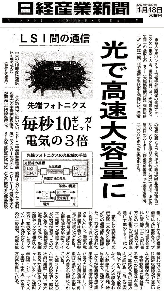
Advanced Photonics ,Inc. has succeeded in developing Photoelectronic Integrated Circuit Design Technology to form optical wave guide in PCB.
Advanced Photonics, Inc.,(APi., Ota-ku, Tokyo, President Mr. Makoto Shigematsu), a venture business company spun off the University of Tokyo and engaged in development of embedded optical wave guide in PCB as well as OE conversion module, has recently announced that it succeeded in developing “ Photoelectronic Integrated Circuit Design Technology” by utilizing combined technologies of optical wave guide manufacturing and interconnection.
APi exhibited Optical Circuit Board with 80Gbps transmission speed in the “8th Fiber Optics Expo” (Organizer: Lead Exhibition Japan) which was held in Tokyo International Exhibition Center (Tokyo Big Site, Koto-ku, Tokyo) from 16 Jan 2008 through 18 Jan. It has been confirmed that the PCB (FR-4 substrate) achieved throughput of 80 Gbps ( 10 Gbps each wave guide) with the epoxy resin wave guides embedded in the board.
APi was established on15 March 2006 on the basis of the research on semiconductors, optical communications and optical interconnection conducted by Prof Yoshiaki Nakano at the University of Tokyo Research Center for Advanced Science and Technology. APi has been engaged in development of basic technologies and their commercialization, anticipating substantial market to take off in 2010. The company is now actively pursuing trial production and development in collaboration with the University of Tokyo.
In January 2007, APi made a prototype PCB which enabled 10Gbps transmission per channel utilizing a technology to embed optical wave guide in PCB, whereby high-speed data transmission was realized between OE conversion modules without using mirror nor lens. According to APi, the wave guide can be produced not only in straight line form but also in curved or branched form.
Advantages of this method without using mirror or lens include fewer man-hour necessary for production which otherwise tends to be larger due to necessity of precision alignment of optical axis, and reduction of the number of parts. In addition, the height of the edge point and OE conversion module can be kept lower, thus enabling more freedom in mounting design and shorter optical path length, which in turn bring about improved signal quality.
APi has already started joint research & development with several leading companies and according to Mr. Shigematsu, president of the company, “ Commercialization of photo-electronic integrated board is achievable by giving consideration to optical wave guides, OE conversion modules and overall design as a system, thereby making optimization of three dimensional interconnection technology and via structures”. (Shigeki Nagae =Producer, Industry Academy Collaboration Office)
Reference site:http://innovation.nikkeibp.co.jp/etb/20080214-00.html
2007/01/21
Our company was taken up by “Tech-On”, a NikkeiBP website, in its electronic parts technology column on January 21, 2008 issue.
Tokyo University Venture has developed Low-cost Photoelectric PCB
Advanced Photonics Inc prototyped a printed circuit board with embedded optical waveguides for use in gaming consoles and workstations, and unveiled it at the 8th Fiber Optics Expo (Figs 1,2). Advanced Photonics is a venture company spun out from the University of Tokyo, which is specializing in optical interconnect devices. The company succeeded in transmitting signals at 80Gbps (10Gbps x eight channels) between photoelectric conversion modules installed on the circuit board. “This method may be less expensive than any other technique announced by companies thus far.” said Mr. Makoto Shigematsu, president of the company.
The cost can be reduced because the method requires a fewer number of components and facilitates the production. In a printed circuit board designed to process both light and electricity, an electric signal is generally converted to light by a photoelectric conversion module before being output to the external waveguide. A mirror or a lens is usually adopted to form the light path even though greater difficulty in alignment cannot be avoided.
The latest prototype eliminates the provision of mirror or lens by utilizing the technology developed by professor Yoshiaki Nakano at Research Center for Advanced Science and Technology at the University of Tokyo. Although the company did not unveil the details of the technology, the improvement was achieved by changing the position of photoelectric conversion modules, which have been normally installed on the board surface. To be more specific, the modules are installed in a recess formed on the board. As a result, the waveguide in the board can be extended vertically from the light receiving/emitting surface without being curbed, thereby making it possible to remove the mirror or the lens.
With the waveguide formed in the circuit board, the density of embedded components can also be enhanced because electronic can be additionally mounted on the positions where a mirror and other parts are located in a board that does not have an internal optical waveguide. Advanced Technology already developed the process technology to manufacture the board. According to the company, the manufacturing equipment used in this technology is quite standard, and no special skill is required for the operator at production.
The company developed interconnect technologies for use not just in a circuit board but between boards. It also designed an optical interconnection with a wiring length of approximately 1m and a certain curvature. The company “ hopes to develop a router with terabit-per-second class throughput in around 2010” by utilizing the expertise accumulated in these experiences, said Mr.Xueliang Song, director and CTO of the company.
Reference Site: http://techon.nikkeibp.co.jp/article/NEWS/20080121/145809/
2007/06/10
An article about our company was taken up by February issue of “O plus E”, a monthly magazine specialized in optics and image technology.
Trends in short range optical communications technology “Expected higher-capacity router and optical backplane” Hitachi, Ltd. Shinji Nishimura, Masato Shishikura
For commercialization of 100Gb Ethernet, challenges are development of optical interface technology which enables 100Gbps data transmission, and realization of higher-capacity router which exchanges large amount of information. This thesis deals with the problems related to backplane through which inner parts of equipment are connected by signals in the routers equipped with 100Gb Ethernet in around 215, and optical backplane technology which may solve such problems. *snip*
Advanced Photonics, Inc. (API) also developed photoelectric conversion module and optical backplane-mounted board. The module developed by API adopts embedded optical waveguide , thus making possible to expect easier maintenance (easier handling) than conventional fiber backplane. Furthermore, the module does not employ the common 45°mirror or collecting lens. According to the company’s report, source and detector device is directly connected with optical waveguide, thus reducing the number of parts and resultant decrease in alignment cost,
The prototype module is as small as 12x15x2mm in size and mounted with source and detector device as well as driver amplifier. With its 4 channels each for transmitting and receiving, the total throughput of 80Gbps was achieved. In the optical backplane board for demonstration, optical waveguides of 32μm in length were embedded in 4 layer FR-4 substrates. The distance between the waveguides is 250μm and the core size of the waveguide is 60μm x 60μm.
Reference Site
http://www.ss-com.co.jp/oe/
http://www.ss-com.co.jp/oe/contents/2007/oe200702.html
 2007/05/31
Our company was covered by "2006 Research Report on Trend in Optoelectronic Technology" (by Optoelectronic Industry and Technology Development Association) in its “ Optical inter-connection ” section ( page 128).
Reference Site : http://www.oitda.or.jp/
For further details, click here (PDF file)
2006/06/01
Our company was featured by Nature, world’s best known science journal in its June 2006 issue which covered venture companies originated from universities.
Japanese spin-offs face struggle for survival
Companies set up by academics are proliferating― but can they secure the investment they need to succeed? Ichiko Fuyuno investigates.
The company, Advanced Photonics, was established in March, and Song is already finding running a business and doing the optics research for product development a challenge. “Stepping into business from the academic world was like leaving for a foreign country again,” he says.
Song is part of a new wave of university researchers in Japan who have been encouraged to set up companies based on their ideas. As part of the government’s efforts to pull the economy out of a decade long slump, it has not just lifted restrictions on academics’ business activities, but is offering them financial backing.
"We can’t support everyone,” says the director of NEDO." The first stage of backing university start-ups is over. Now we’ll only take care of competitive companies.”